Custom design DW1000 RF problems

Hello Gentlemen,

This is my first post on this forum, so if the information which I’m supplying is not sufficient, please let me know.
Currently I’m working a custom implementation of the DW1000. This implemenation is currently in the testing phase and sadly I ran into some trouble.
For the custom design I followed a lot of the design guides (which are very helpful). To make sure that the assembly of the PCB would remain within budget I designed it with mainly 0402 components and the PCB to be manufactured at JLCPCB. The external clock of the DW1000 is supplied by an external clock generator.

After manual assembly of two prototypes it was discovered that the DW1000 communicates with the MCU as expected and is mostly operating properly. The part which is not working is (presumably) the matching of the antenna.

Up to this point I’ve had zero communication with any external devices. The DWM1001 is used to send and receive messages. Why the messages are not being received or transmitted by the custom design is unclear. For testing I used two antennas:

  • WB002 of the DecaWave reference design

  • Taoglass Limited FXUWB10.01.0100C

Both antennas don’t work, very likely due to bad impedance matching on the PCB. This is where I’m not sure. During the design phase I’ve put quite some emphasise on the correct matching of the RF traces. I use a four layer PCB, with the RF traces matched with the internal ground plane as a reference.
Sadly I have no VNA to test the traces at the UWB frequencies, so I’m very much in the dark right now.
By this post I hope that someone might be able to spot the problem in my design. Due to the 0402 components it certainly ain’t perfect, but I don’t see why it wouldn’t work.

Here you can see the board layout with the solid ground plane right below it as the reference:

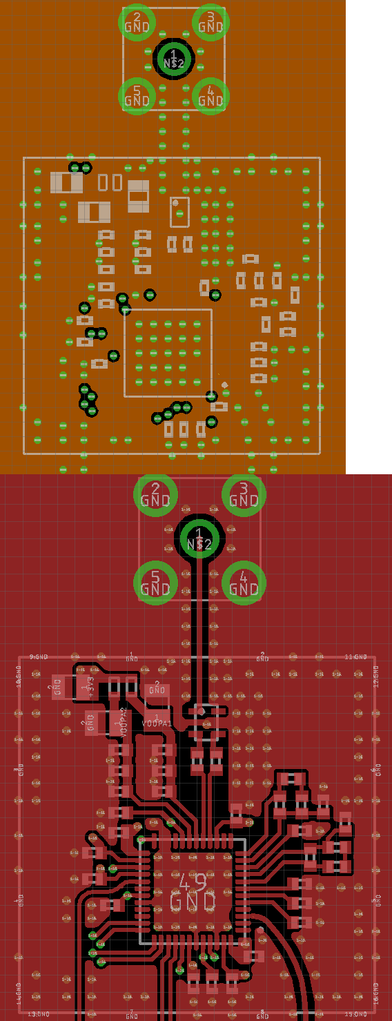
The width of the 100 ohm differential traces is 0.2mm, the width of the 50 ohm trace to the SMA connector is 0.293mm (11.55mil). The traces are 7.1mill above the internal ground plane.

Hopefully I’ve now supplied a sufficient amount of information for someone to spot the problem.
It’ll be very much appreciated!

Thank you,
Glen

1 Like

I’m the software developer and work with Glen on this project. Just in case anybody needs the info, here’s the used radio settings:

const RADIO_RX_CONFIG: RxConfig = RxConfig {
    bitrate: BitRate::Kbps6800,
    frame_filtering: false,
    pulse_repetition_frequency: PulseRepetitionFrequency::Mhz16,
    expected_preamble_length: PreambleLength::Symbols128,
    channel: UwbChannel::Channel5,
    sfd_sequence: SfdSequence::IEEE,
};

const RADIO_TX_CONFIG: TxConfig = TxConfig {
    bitrate: BitRate::Kbps6800,
    ranging_enable: false,
    pulse_repetition_frequency: PulseRepetitionFrequency::Mhz16,
    preamble_length: PreambleLength::Symbols128,
    channel: UwbChannel::Channel5,
    sfd_sequence: SfdSequence::IEEE,
};

These should be the same as the default.

Hi Glen,

I wouldn’t anticipate that bad matching can be a reason for no communication in your case. The impedance looks close to target 50/ 100 Ohms. What is the gap between 100 Ohms tracks?

What MCU is used?
Can you also share a schematics of the DW1000-related part? Power, data interface, RF part.
Do you see a DW1000 interrupt after TX?

Hello Alec,

Thank you for your swift response.
The MCU which is used is the STM32H753, which is quite a powerful microcontroller.

The clearance between the traces is 5mil.
Here you can see the schematic:


@diondokter247 can you give an answer on the interrupt after TX?

@alec @glen

Yes, the TX does generate an interrupt and makes the TX LED blink.

One thing that might be interesting is that on the lowest bitrate in channel 1 and the longest preamble, that sometimes the radio will report an RX SFD error when a message is sent from a DWM1001C (with the same settings of course).

edit: Also tried using a really slow SPI speed of 500 khz. Changed nothing.

Hi Glen

I’m not an expert, but I see quite a lot of issues with this design:

  • The clock source trace seems to be pretty long, coming from outside your shield can. I suggest placing the clock source closer to the DW1000 and placing it under the shield. What sort of clock source are you using?
  • The SMA connector you are using is not the best choice. It makes a stub and adds a big pad creating a discontinuity in the antenna trace. An edge mount SMA connector is suggested, see section 7.2: SMA Connectors in APH0001: DW1000 hardware design guide
  • The decoupling caps are quite far away from the pins. I suggest using 0201 components so they can be placed closer to the IC.
  • The antenna trace seems longer than it needs to be. Try to keep it as short as possible
  • I suggest placing a GND plane around your differential antenna traces, with vias on both sides. Place a via closer to pin 2 of you balun. Imagine a return current coming from pin 4 and 5 of the SMA connector, that will favour travelling underneath your antenna trace. It needs a low impedance path to pin 2 and 5 of your balun. mirrir your VDDPA1 decoupling caps.
  • You need more vias to stitch your ground planes together, especially near the edge of your board.
  • The decoupling capacitor of VDDIO is placed sub-optimally

I suggest contacting our sales team so our apps team might have a proper look at the design. I understand uploading the full schematic and design on a public forum might not be feasible, but having more context would be helpfull.

Hello @seppe,

a week ago, on the 4th, we’ve sent an email about this.
But so far we’ve had no response.

Hopefully you can get back to us.

Hi Dion,

Sorry, was too busy last weeks.
I didn’t find any big issues wrt schematics.
I’ll come back soon with some suggestions.

1 Like

Hi

Could you tell me the email address you sent this enquiry to and what company this was for? I don’t see anything in our internal ticketing system.

Note that “official” design reviews are typically assigned by our sales team. We would love to support every single customer with their design, but in practice we have a limited bandwidth so we can’t handle every request. I hope you understand that as a company we have to prioritise on projects that bring us the most business or opportunities.

This forum allows us to work on more of a “best effort” basis and to allow our customers to help each other. Also note that I typically do not do hardware design reviews, I just shared what I know based on our documentation.

We have a lot things going on and a limited bandwidth, so there might be some delay on a full review.

Thanks for responding!

I understand that you have a limited bandwidth. The used email address was from tehofsteengineering.nl and sent by Glen.

If you want to know the business opportunity, we’re currently in the prototyping stage.
This will consist of ~40 DW1000 radios in some form.
If the prototype is a success, then a further roll-out of a few hundred radios is likely to follow.
Then if the system is liked throughout the company and we’re starting to rely on it, then it will be a few thousand.

Can’t give guarantees of course, but I’m doing my best to to make the project a success.

Hello Seppe,

I understand the bandwidth limitations during these challenging times.
Currently I am layouting an updated version of the design, however this is somewhat difficult since I still did not receive a response on my email. I did receive the confirmation email from the sales team after sending it, so everything should be fine on that part.

Personally I suspect that the PCB technology I’m using is not up for the job. The current PCB’s are manufactured with ENIG-RoHS surface finish and FR-4 TG155.
I’m considering to switch to (more expensive) Rogers RO4350, but before I do this I would like to see my designed received.

We really want to get the DW1000 to work in the upcoming batch!

Hi glen

Most if not all of our designs use FR4 PCBs. With modern manufacturing processes a tight enough tolerance can be achieved for successful impedance matched designs at the used frequenies. See appendix 1 in APH006 for an example stackup.

I would suspect the main issue being the clock source. We typically use a 38.4 MHz “room temperature crystal oscillators” (RTXO). We also tested TCXOs but these tend to be more expensive and can introduce phase noise, which is why we tend to stick to and recommend RTXO for most applications (a TCXO or OCXO might be beneficial in certain temperature environments). See also section 2 in APS011.

I suggest looking at the center frequency when transmitting a continuous wave. If there is an offset that is too great (>50-100ppm, depending on the antenna, range, …) UWB communication will not because the link budget is greatly reduced (not to mention ranging accuracy will greatly decrease).
You seem to use a different solution, and the trace length looks very long which could result in noise being coupled in and a load capacitance that is to high for you clock source.

The CFO (Center Frequency Offset) can be measured with a spectrum analyser or a frequency counter.

I suggest having a look at my previous comments. Imperfections in the antenna path such as the right angle SMA connector will increase insertion loss, and thus lower the link budget and potentially increase spurious noise. This is not optimal, but typically UWB communication and even ranging should still be possible. The max distance will typically be lower, ranging accuracy will decrease and meeting certification becomes difficult.

Alec is having a look at your design. He has more experience than me in this and if I understand correctly he has access to the full schematic, so he should be able to provide better feedback.

Things can go horribly wrong with such a setup in ways that remain undetected. The DW1000 clock source is super critical, you can’t just use any clock to drive it.

The only viable clocks we see work on DW1000 are crystals and TCXOs. Any device based on a PLL clock generator usually fails, creates too much jitter or phase noise in the clock signal for the DW1000 to operate properly. The boards will appear to operate properly in every respect except the packets just don’t seem to get to the other end.

I suggest, as a test if nothing else, that you replace the clock generator with a 38.4 MHz crystal on your board. If the crystal works, then you know the clock you were providing is bad.

Also, when using an external clock source into XTAL1, you must protect VDDBATT from voltage spikes. The recommended way to do this is to LDO the supply voltage down to 3.0 volts. This is what is shown in the DW1000 documents.

That is consistent with a bad clock, everything “works”, but no signal gets through.

Note that a bad match in the antenna won’t disable short range reception, say under 1 meter. So if you can’t get any signal across at short range, it isn’t an antenna match problem.

I doubt that. The worst antenna match in the world will work at short range. At some range, say under 50 cm, the boards will communicate with no antenna installed, just the SMA connector open. Can’t be any worse match than that.

There are a number of other issues in the design, but most that I see shouldn’t prevent basic operation.

Mike Ciholas, President, Ciholas, Inc
3700 Bell Road, Newburgh, IN 47630 USA
mikec@ciholas.com
+1 812 962 9408

1 Like

Thanks a lot for your insight Mike. I don’t have any experience with clock sources other than crystals and TCXOs. It sound like you did more research on this.

Glen, you might want to check the RF Status Register, see section 7.2.41.1 in the DW1000 User Manual.

Especially the RFPLLLOCK bit could be of intrest. This bit should indicate whether the RF PLL is locked. Note that it might still be possible for this PLL to be locked even if the clock source has a frequency offset or phase noise, and the PLL can switch between lock and unlocked status if the clock is unstable.

Thank you guys for the support. I’m happy to say that we fixed the problem.
As you suggested the clock source is of major importance. Initially I was not questioning our source, since it appeared to be very clean on the oscilloscope.
We did however, drive it on a voltage of +3V3 which is as we found out, often too high for the DW1000 to properly capture.
Also the VDDBATT was not “isolated” from the noise on the +3V3 line by using an LDO.

Currently I supply VDDBATT with +3V from an LDO. This +3V I also use for a TCXO which I hacked in place instead of the PLL. This setup is now working. Great!

Most of the other design improvement you guys suggested have also now been implemented. I’m quite confident that the next iteration of the PCB will be successful.

Again, thank you for the help!

It seems we’re not the first ones to run into this problem. Maybe it’d be a good idea to write a little bit more about it in either the datasheet or the user manual.