DW1000 IC PCB Design - XTAL1 PIN - TCXO

Hello,

I have a question regarding the DW1000 IC in combination with a TCXO and would be forever grateful if Decawave or someone else could comment on this question.

I would like to use a TCXO in order to drive the DW1000.

It has already been discussed in this thread that the data sheet does not mention the input impedance of the XTAL1 pin:

The only information regarding the requirements for an external clock given by the date sheet is shown below:

Decawave can you tell use the input impedance (R & C) of the XTAL1 pin?

The datasheet recommends the TCXO “ASTXR-12-38.400MHz-514054-T” which has an output load impedance of 10K || 10PF.

Is 10K || 10PF the input impedance of the DW1000 XTAL1 pin?

I also would like to know if the DW1000 can be driven by LVCMOS instead of clipped sine wave?

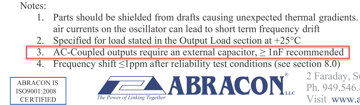
In addition, I saw that ABRACON recommends an AC coupling capacitor with a value larger than 1nF:

Decawave recommends to use an AC coupling capacitor of 2200pF.

Why exactly this value?

I saw that some TCXO manufacturers recommend an AC coupling capacitor of 0.1uF.

Which value should be used in this case?

How can the value of the coupling capacitor be properly determined?

Will a value of 0.1uF which is much larger than the recommended 2200pF do harm?

Lastly, I also saw that some manufacturers recommend a termination resistor, but I don’t think that this is really necessary if the TCXO is right next to the IC. What do you think about this ?

Kind regards
firstdragon

1 Like

It will be quite high, a few pF capacitance (~4 pF), and very high input resistance, maybe > 1 megaohm, biasing it to some mid range voltage.

The 10K || 10 pF is a test load used to establish the TCXO performance, not a measure of the actual load it expects, or even a required load.

No.

Yes, it can. Suggest the LVCMOS signal also go through a DC block cap. Be careful not to overdrive the signal as this can lead to degradation in the system performance. Best way to check is to put DW into continuous wave (CW) mode and observe the carrier with a spectrum analyzer. You want a sharp narrow peak with few to none side lobes and spurs. Spurs are caused primarily by noise on the XTAL1 input messing with the PLLs.

The quality of your clock source on XTAL1 is paramount to achieving good UWB location performance. Any sort of jitter or noise on that signal can ruin your performance.

That is mostly arbitrary, just has to be high enough value to not meaningfully affect the signal amplitude. At 38.4 MHz, 2.2 nF is under 2 ohms impedance, which has no measurable affect on the signal amplitude.

No, though it might slow down initial start up a bit as the cap establishes DC bias on both sides.

This will depend on your layout. A long PCB trace to XTAL1 can cause reflections and that can lead to issues (which will be evident in the CW test).

Generally, the best method is a series resistor at the driving end equal to the PCB trace impedance, so called “series termination”. This uses the least amount of power and causes the least loss of signal amplitude. Parallel termination at the end of the trace is possible, but consumes power and causes loss of amplitude, some of which can be mitigated by AC termination techniques.

A decent article on termination techniques:

Mike Ciholas, President, Ciholas, Inc
3700 Bell Road, Newburgh, IN 47630 USA
mikec@ciholas.com
+1 812 962 9408

1 Like

Thank you for this insightful answer.