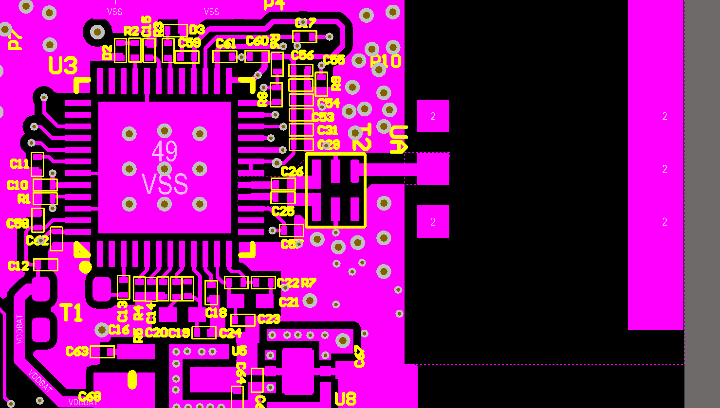
We recently made a design by changing the VDDBAT pin and TCXO to 3.0 volts.The LDO is TPS73601 which converts 3.3 volts to 3.0 volts,and the TCXO is ASTXR-12-38.400MHz-514054-T.The PCB layout with the solid ground plane right below it as the reference.The problem is that when we test this board the Packet Error Rate is almost 60%. So is there any mistake in this design? Does anyone have any suggestions about the TCXO design?
regards,
Boboy2011
Hi~.
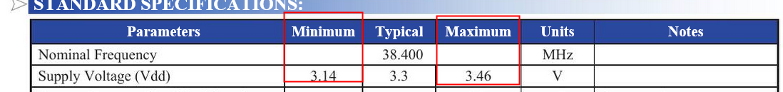
The standard of TCXO you choose is available only within 3.14~3.46.
Have you checked this out?
Did this same board design work before switching the TCXO and voltage source?
Because looking your layout my first thought is that your power connections to pins 18 & 19 (VDDPA1 and VDDPA2) are exactly what the layout guides tell you to avoid doing because it will cause distortion in the output transmissions.
Thank you very much for reminding me! I have another question is that in DW1000 Datasheet.pdf,the optional external pull-ups for SPI mode configuration is showing like this:

My question is that should the point which pointed by red arrow connect to GND, and my schematic diagram is showing like this:
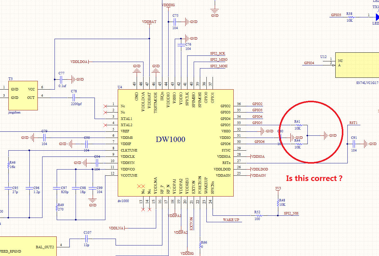
Is this correct? thank you!
No, that is incorrect. The decawave schematic is admittedly rather confusingly drawn but shows the pullups connected to VDDIO not GND.
But it does depend on the SPI mode you wish to use. The way your schematic is drawn you will get SPI mode 0. The way the decawave schematic is drawn they will get mode 3.