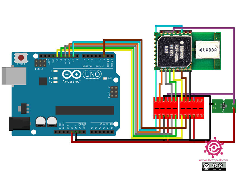
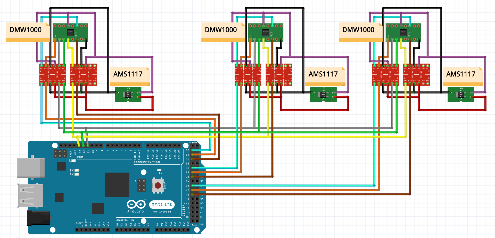
The DWM1000 has 4 SPI connections, CLK, MISO, MOSI, and chip select.
The CLK (yellow), MISO (green) and MOSI (grey) can be common between multiple modules, the chip select (orange) needs to be unique for each module. The module also has an interrupt output (brown) which should ideally be different for each module.
Your diagram also shows GPIO7 from the module connected up (the light blue/cyan line). Without digging into the arduino driver you’re using I’m not sure why this line is connected and what function it could be serving, you shouldn’t need it. Whether it can be common or not depends what it’s being used for.
The MISO line (master in, slave out or data from the module to the processor) should be combined before the level shifter circuit rather than after it. The outputs from the modules won’t be driven unless the module is selected but the output from your level shifter could well be driven all the time resulting in a conflict if you connect two outputs together. Other than that and the uncertainty on GPIO7 I think your diagram should work assuming the power output on the uno is up to the job of running 3 radios.
I should add that I’m not that familiar with the arduino platform so take all of this with a pinch of salt.
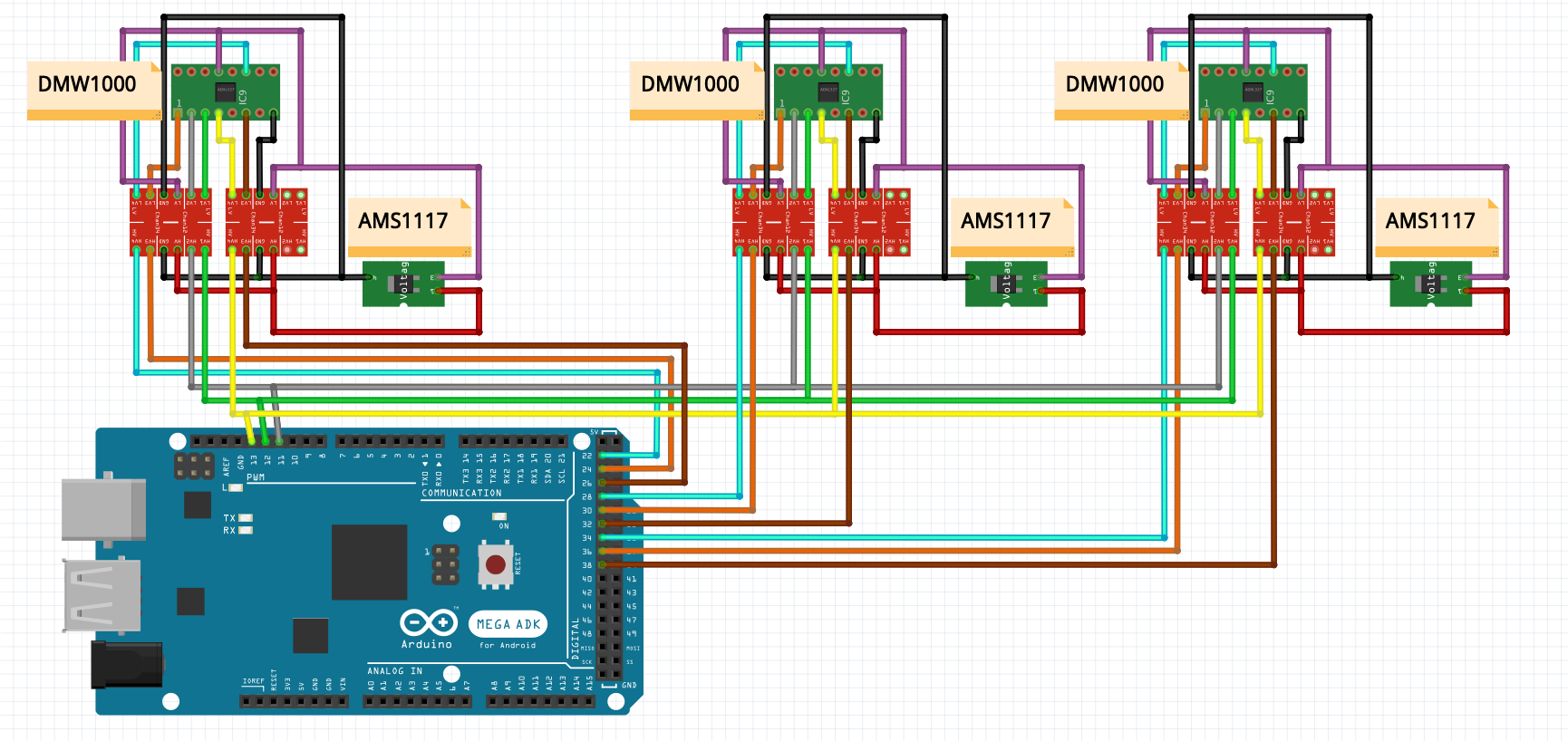
Thank you very much for your help. I modified the diagram according to your indications and made it easier to understand. Tell me if I have any errors, please.
I share the yellow, green and gray pins.
The tutorial says that it is the reset pin (PIN_RST), I placed it although I do not know what it is for, but it is in the code. cyan color, pins 22, 28, 34.
I have the PIN_IRQ brown line connected to pins 26, 32, 38
The orange line I don’t know what it is for, it is not defined in the code, it used to be on pin 10. I think it is the CS, but I don’t know exactly what it is for or where it goes. You told me it’s separate. pins 24, 30, 36
OK. Looks like I miscounted the pins
You could probably get away with a common reset pin for all 3 modules if the driver only uses it on startup but if you have the IO on the processor then one per device is the safe way to do it.
The orange line is indeed CSn (the n (short for not) just means it’s active low rather than high, this is common for most chip select and reset lines). Most chips designed to go onto a shared connection to the processor will have a chip select line. When a chip is selected it will listen / reply to the processor, when it isn’t selected it will ignore the lines from the processor.
This line should be high most of the time and then go low for one DWM1000 at a time as you want to talk to them. On SPI the chip select is also used to indicate the start and end of each read/write command. If more than one is low at the same time they will try to all talk at the same time on the MISO line this is 1) not good for the parts and 2) will result in you receiving junk data.
You still have the MISO line common after your level shifting boards. You should common these before the buffers. The modules will only drive the MISO pin when chip selected, the buffers will drive them all the time.
The arduino Mega has a lot of pins so it doesn’t cost me a thing to fit a reset one for each one. I’ll leave it as is if it’s the safest way to go. That is, pins 22, 28, 34.
I don’t understand this part, honestly. Excuse me, I’m a little new to this.
I have 3 questions that are not clear to me:
1- What should I do with the MISO line (green)? (The last thing you said is not clear to me, as I told you).
2- The orange line, is it okay where it is? You say it’s CSn, but it’s not clear to me where it goes.
3. The brown line, is it okay where it is?
Electrical signals are a one to many system. You can connect lots of points together allowing lots of different parts can receive the same signal. But you can only ever have one device driving the signal on to that a wire at a time.
If two different parts are trying to output a signal onto the same wire at the same time then you get what is called a conflict. The two different outputs fight each other as they both try to set the wire to the voltage they want.
This is not a good thing and should be avoided.
On an SPI bus the CLK and MOSI (master out, slave in) pins are driven by the processor and go to all the devices. The MISO (Master in, slave out) pin is the input to the processor can can be driven by any of the connected devices. In order to avoid a conflict on this wire each device will only ever drive its MISO output if it is chip selected.
Each device has a chip select input, when this is active it will listen for data on the MOSI line and will output data on the MISO line. When chip select is not active it will ignore the MOSI line and will not try to output anything on the MISO line (in electronics terms the pin is said to be in a tri-state or high impedance mode).
So you can connect all of the MISO pins together as long as you only have one chip select active at a time.
But arduino is 5V and the DWM1000 is 3.3V which is why you have a level shifting buffer between the two, this converts the voltages between the two parts. Unlike the DWM1000 modules these buffers don’t know when a module is selected and should drive the line to the processor and when it isn’t selected and so shouldn’t drive the processors MISO line. This means you could get a situation where two different buffers are trying to drive the MISO wire at the same time.
The best way to avoid this is to only have one buffer driving the MISO line, that eliminates the problem. So you connect all of the MISO lines from the DWM1000 modules together directly (where we know only one will be driven at a time) and then connect this combined signal into the buffer that increases the signal to 5V and sends it on to the ardunio.
Yes, CSn looks OK. This can come from any pin as long as you only use one at a time which the driver should take care of. If you wish to use this hardware setup but run software that only uses 1 or 2 of the modules then ensure you set the unused CSn lines high.
The brown wire is the interrupt signal from the radio. This is used to indicate that the radio needs to talk to the processor. On most systems this would go to a pin that could be configured as an interrupt input but arduino tends not to use interrupts and will probably just be polling this pin. In that situation any IO pin will work fine.
I want to thank you very much for all your help and explanation.
Cables confirmed to be well connected:
CS (orange) - unique for each module, pin 24, 32 40
Reset (cyan) - unique for each module, pin 22, 30 38
CLK (Yellow) - shared by each module, pin 13
MOSI (Gray) - shared by each module, pin 12
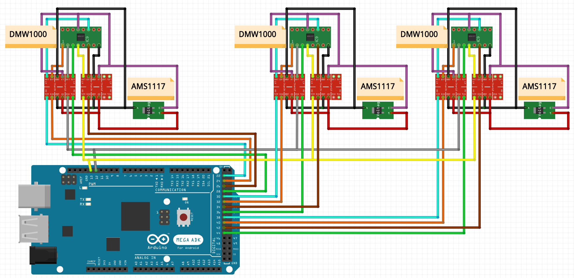
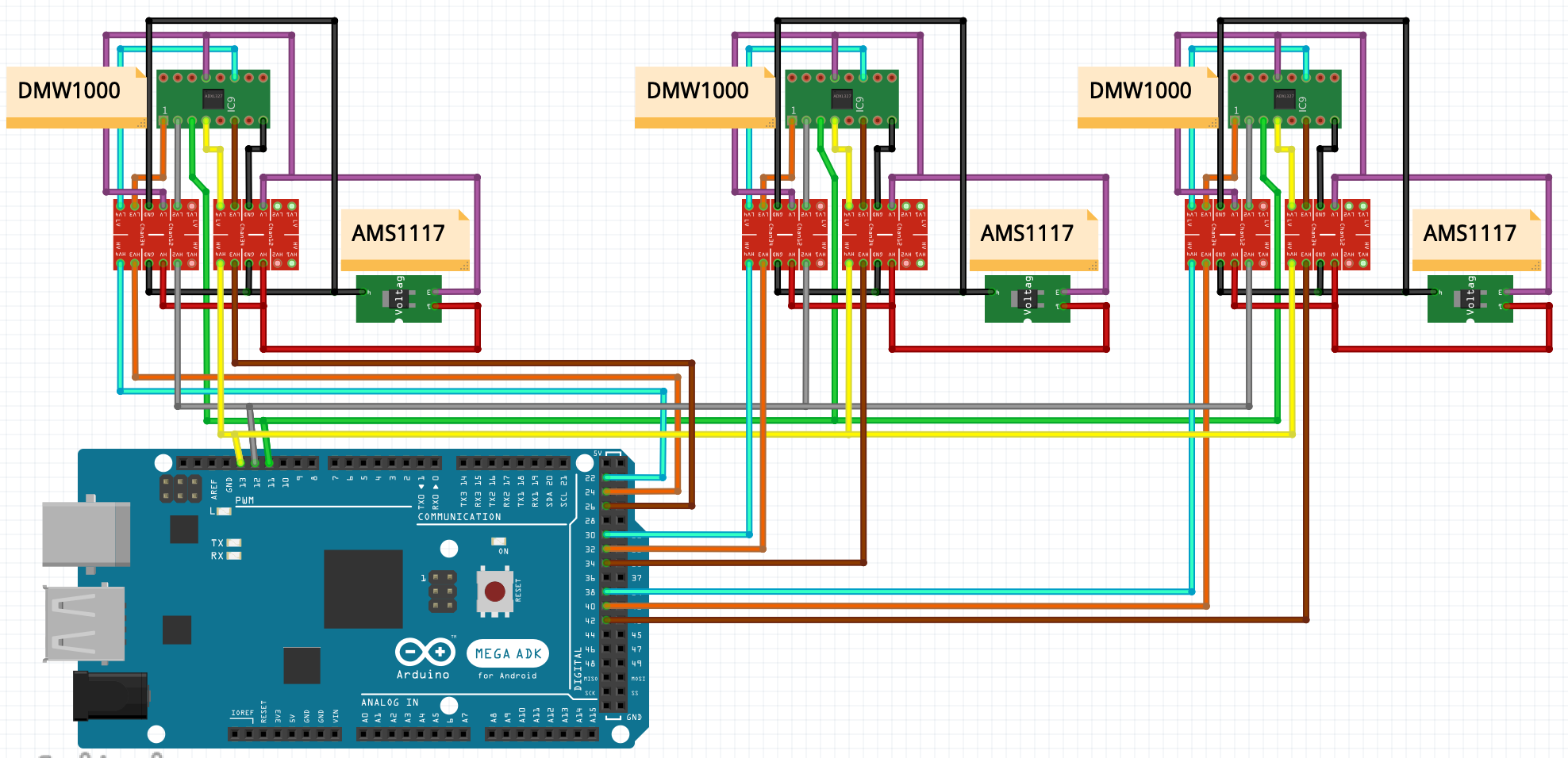
The only one I don’t understand is MISO (green). I have two alternatives (in the diagram I only change the connections from green), tell me which one is correct, please.
Look at how that is now, I think this is what you mean. I will be grateful if you explain to me in a simple way why to put it like this, because the tutorial on the page says to connect directly to the Logic Level Converter (the two red cards in the diagram).
No. Connected the combined signal to the logic converter. Although a 3.3V signal will probably work fine into the Arduino you may as well use the logic converter since you have it there.
You do it like that so the signals are combined in a way that doesn’t create a conflict. I’ve already explained the reasons for this, you can’t have two different things driving the same wire and the logic level converters don’t have any way of knowing when they are supposed to drive the signal and when they aren’t.
A thousand apologies for asking the same question, I sincerely hope you do not bother after all the help that you have given me without interest.
But, it was not 100% clear to me, can you tell me where to put the 3 green wires exactly? I am inexperienced trying to learn and not burn the module in the attempt.
Join the three green wires from the DWM1000s together as soon as they come out of the DWM1000 modules.
After that connect that single combined wire to a level converter and the arduino in the same way as you did in your single DWM1000 setup.
Tell me which of the two is correct, please. I don’t know if you mean: Case 1 as I had it before (all MISO with their logic converters and then to the arduino). Case 2 (all MISO to one logic converter and then to the arduino). (Just look at the green line it’s the only thing that changes)
Thank you very much for your answer (glad to know that I already have the diagram ready), but why is that the correct way? What do you think would happen if everyone had their own logical convert? Where would it go wrong?
I read that these DWM1000 modules have their own communication. My question is: is it possible that they don’t reach out to everyone? That is, 3 anchors and 1 tag joined and unique, not to be confused with another tag.
Is it possible to key them or something like that?
That is purely down to the radio protocol used.
The radios will send to anyone listening and, assuming they are in receive mode, receive any messages sent with the correct radio configuration. Whether you pay any attention to the messages received or not is purely up to the firmware.
There is an optional hardware filter you can activate that can be used to make the receive logic reject any packets that don’t meet a certain criteria but I’ve never used it and so not looked into it in detail.
So you can in a way pick what to receive but you can’t pick who to transmit to, anyone with the correct settings will be able to pick up anything you send.
(I bought it because the dwm1000 modules already arrived and their pins are very close together for the breadboard, rookie mistake, and I don’t want to do a bad soldering with wires).
What changes from the diagram above? Do I no longer need the Logic Level Converter or is it necessary? I want to have everything ready for when the adapters arrive.