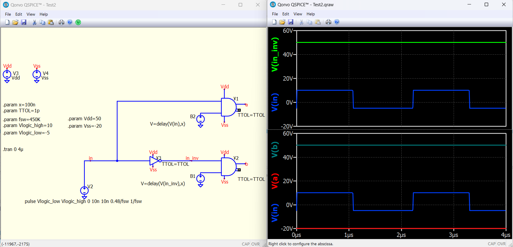
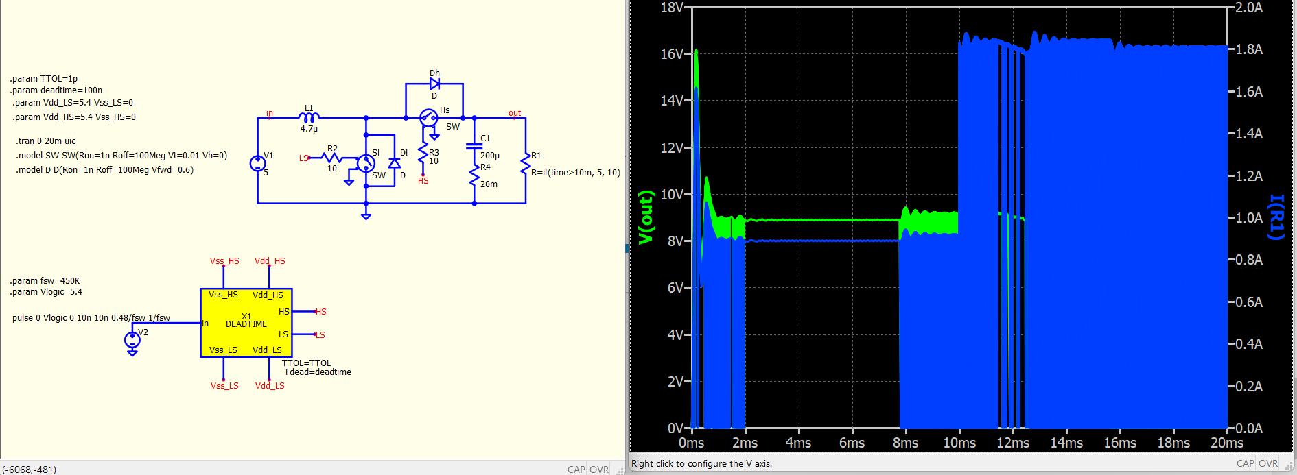
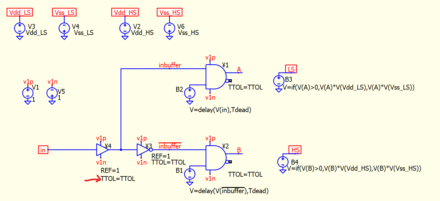
I want to have at the output the square wave signals for a and b but having the positive amplitude Vdd and the negative amplitude Vss, independent the values at Vlogic_low and Vlogic_high. Also, it is not allowed to supply any of the 3 gates with Vlogic_high for Vdd and Vlogic_low for Vss. Is it possible such a thing? Test2.qsch (8.2 KB)
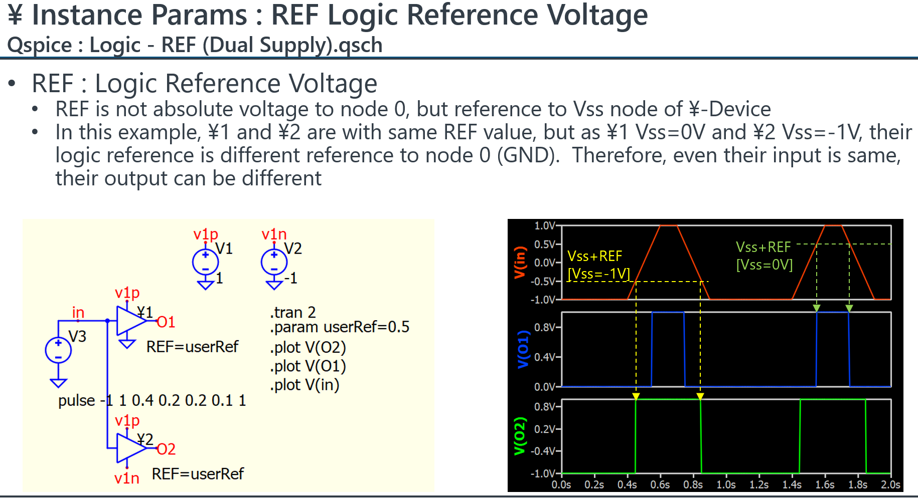
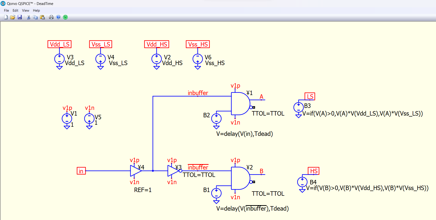
Switching voltage for logic gates is (Vdd+Vss)/2 in this case switchig voltage is (50-20)/2 = 15 V, you can set reference voltage in attributes like REF=5 or change Vlogic high or low.
Ivan1, I tried already this before posting. I think the problem is much more complicated than that. I was able to find particular cases where works, but right after I changed the value for Vlogic_high and Vlogic_low then the things mess up and start to not work anymore. But If You found a way You can post your solution.
The idea is this: I know that V2 will be a square wave signal having let’s say some unknown value for positive amplitude (Vlogic_high) and some unknown value for negative amplitude (Vlogic_low). Therefore whatever values will have Vlogic_high and Vlogic_low at V2, I need to be able to set the positive amplitude and negative amplitude for a and b square waves independent of values of Vlogic_high and Vlogic_low.
I thing that this problem does not have a solution, at least for the shown circuit. That’s why I posted this problem to see other people thinking.
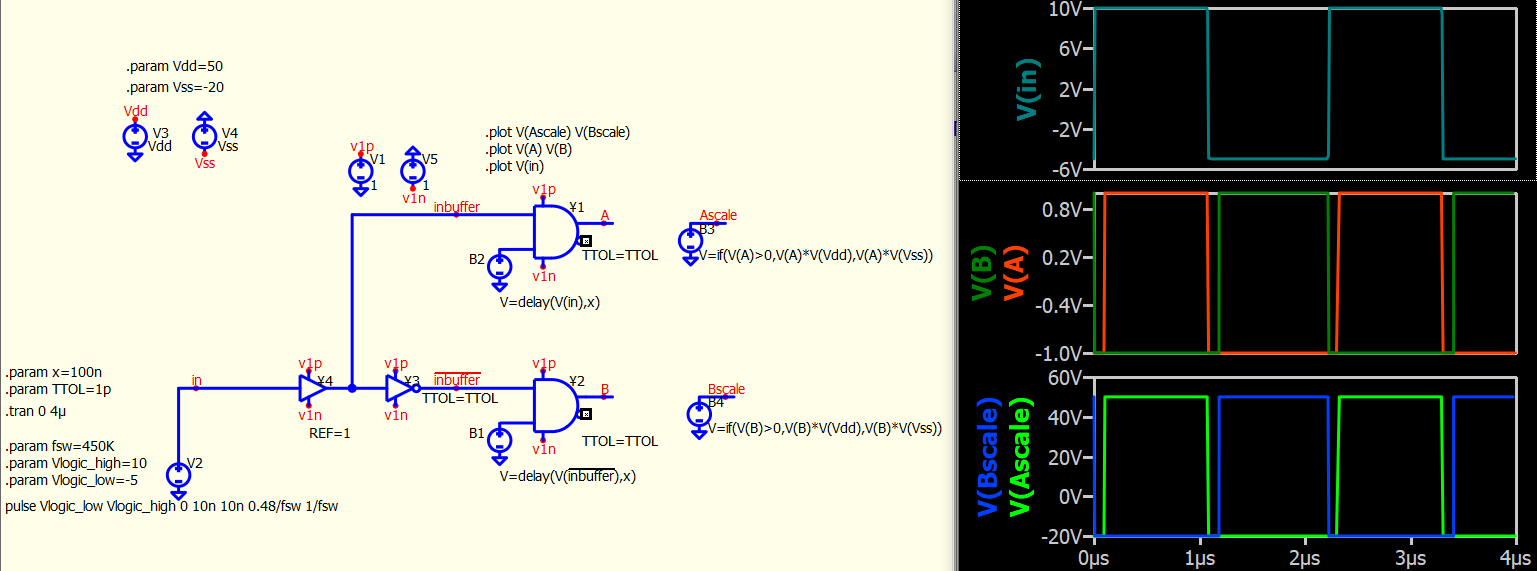
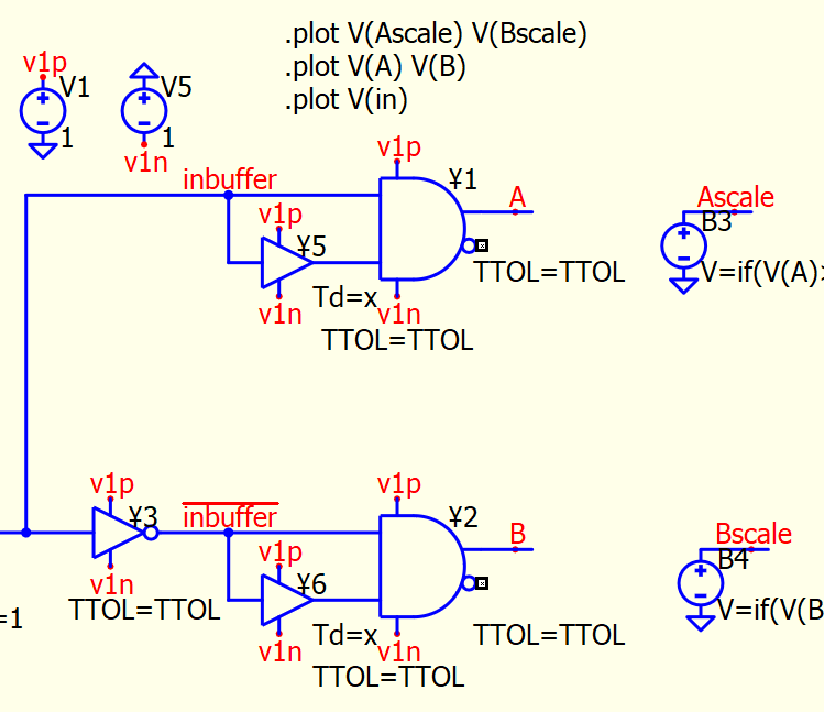
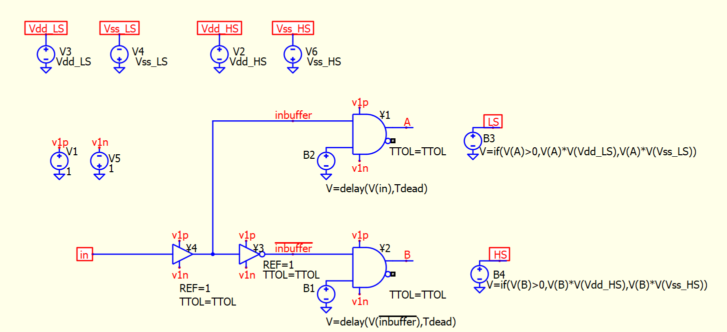
This is the solution I can think of. Force the logic level to +1/-1 (I set input buffer with REF=1, where logic threshold is at 0V, you must determine where is logic input threshold). With logic at +1/-1V, you can scale your output with a B-source and if condition.
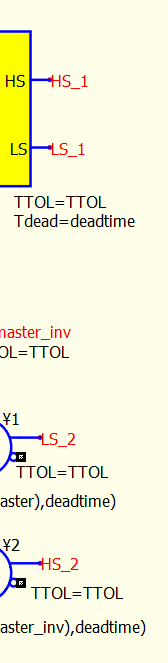
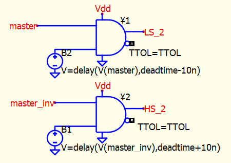
Just a remind, you are working on creating deadtime. If you have no plan to change deadtime during a .tran, better to use buffer with Td than B-source with delay.
How to think about this REF associated with logic gates? Could you live more explanation about it? Its a threshold that does Something inside the gates? What does this REF attribute? And this REF attribute has effect only in the case of logic gates, right?
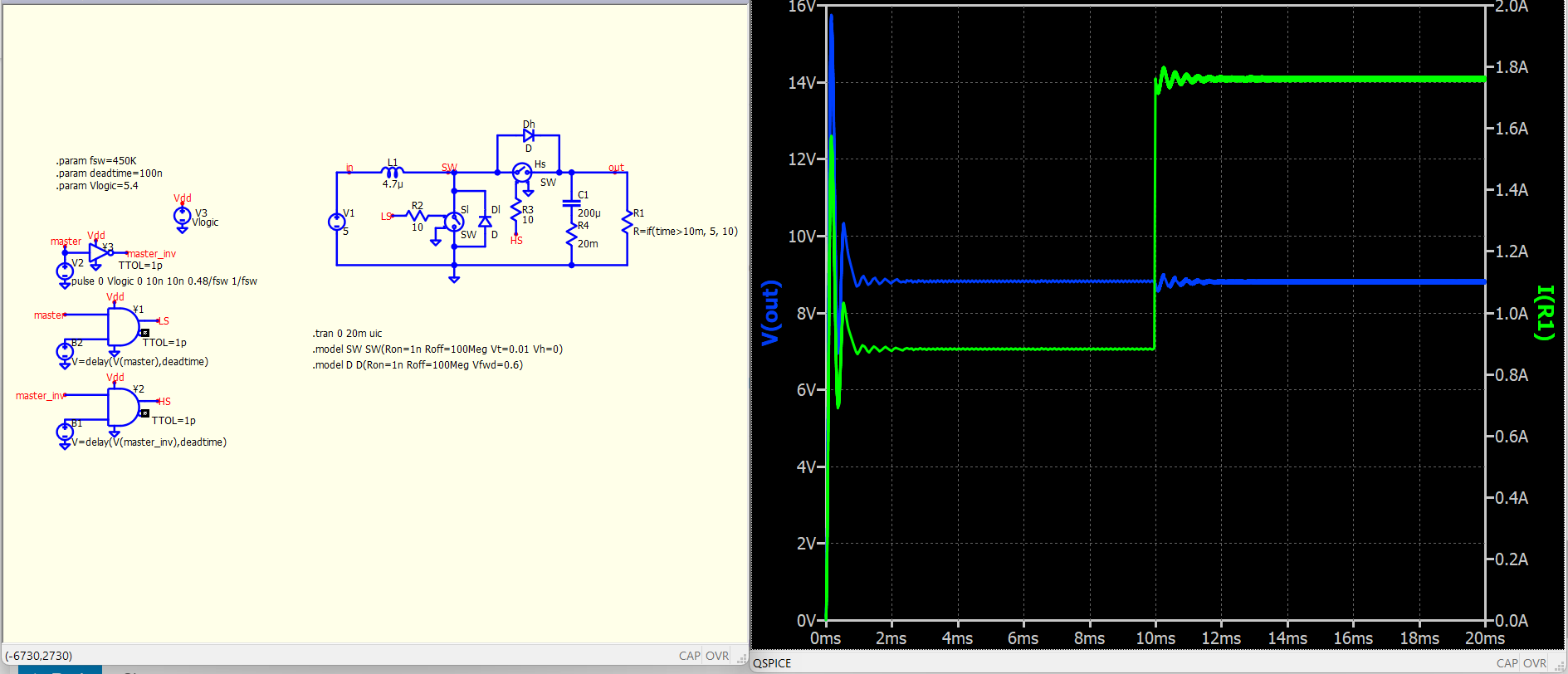
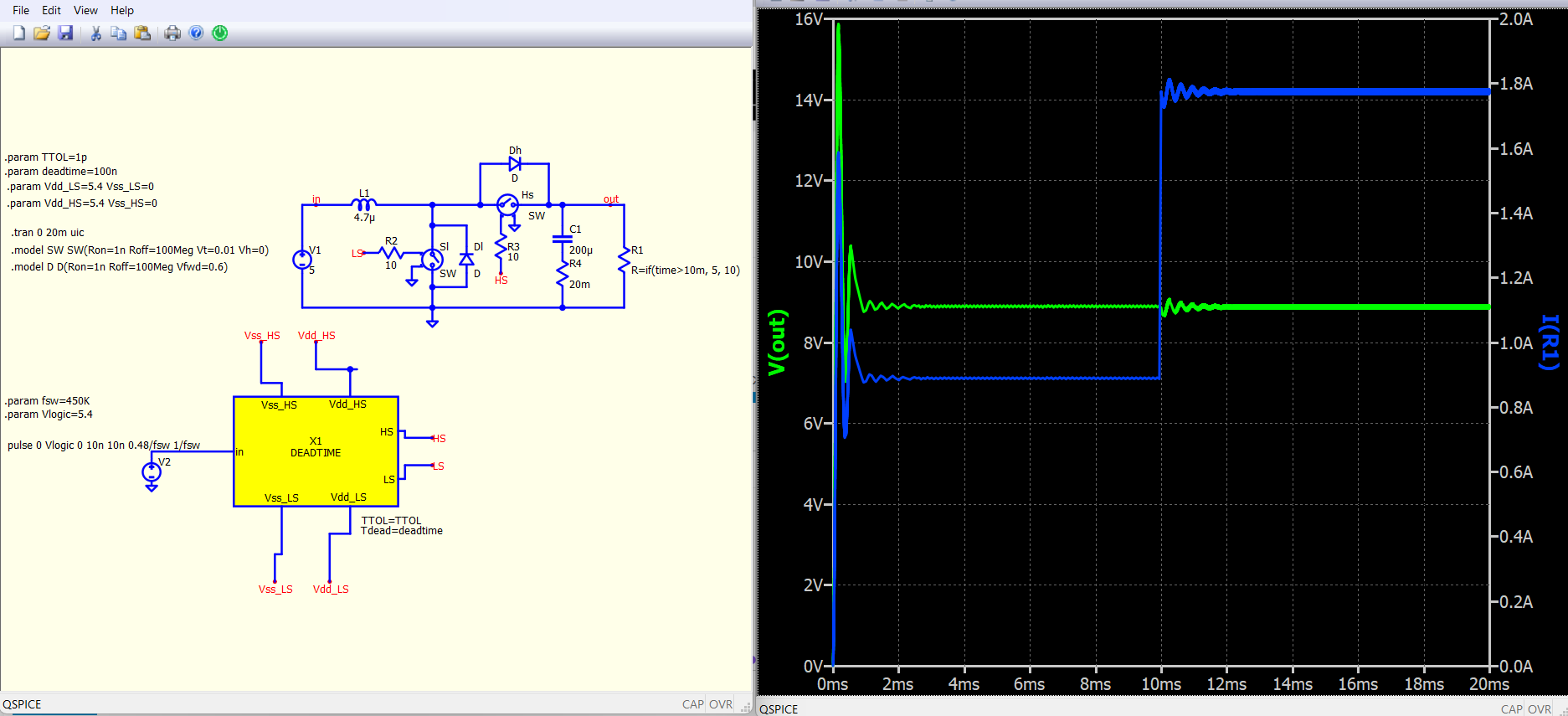
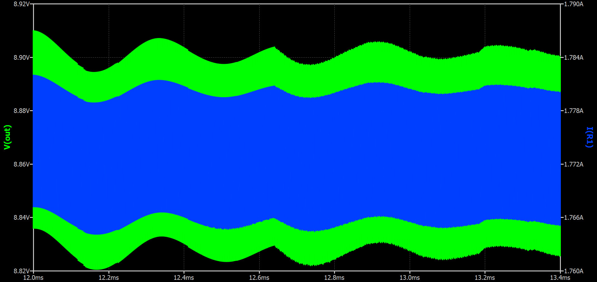
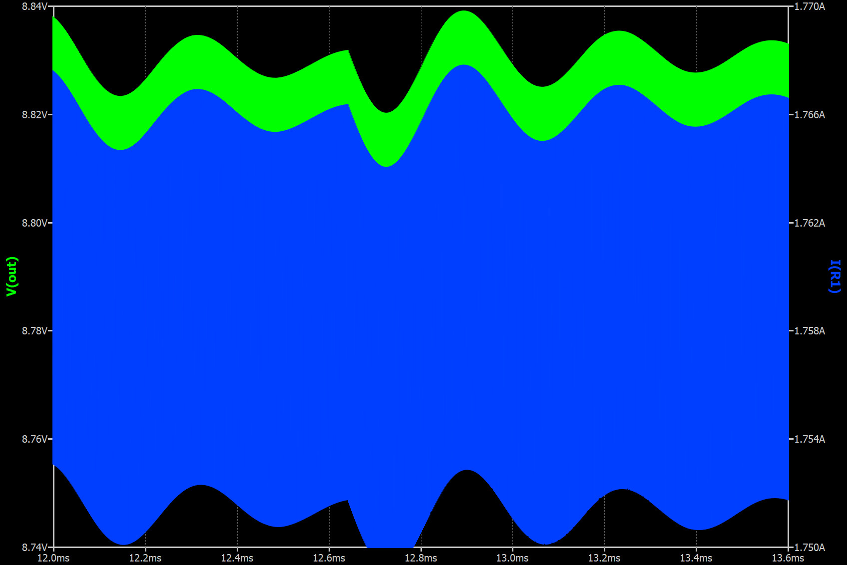
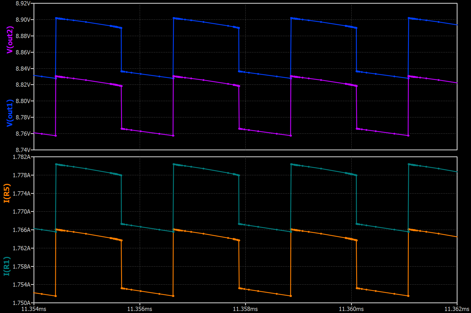
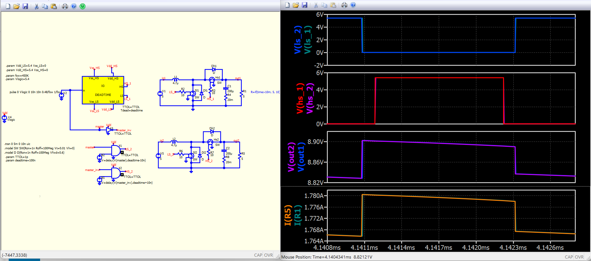
The 2 schematic should have the same results…there is a slightly but noticeable difference…
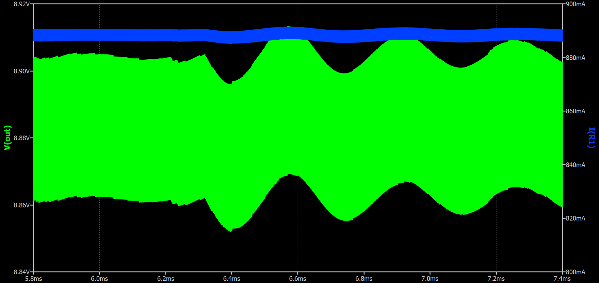
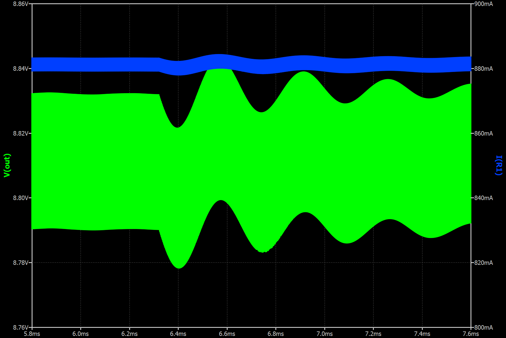
Below is with R1 = R5 = 5R (constant value). This difference for sure matter…and is not good as this difference exist. They needs exactly match…
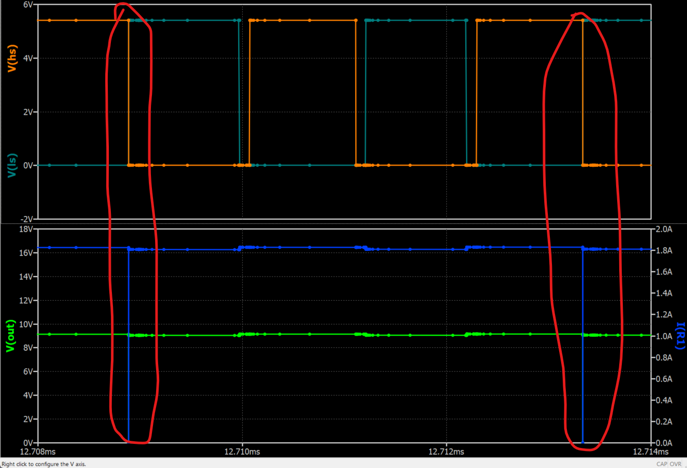
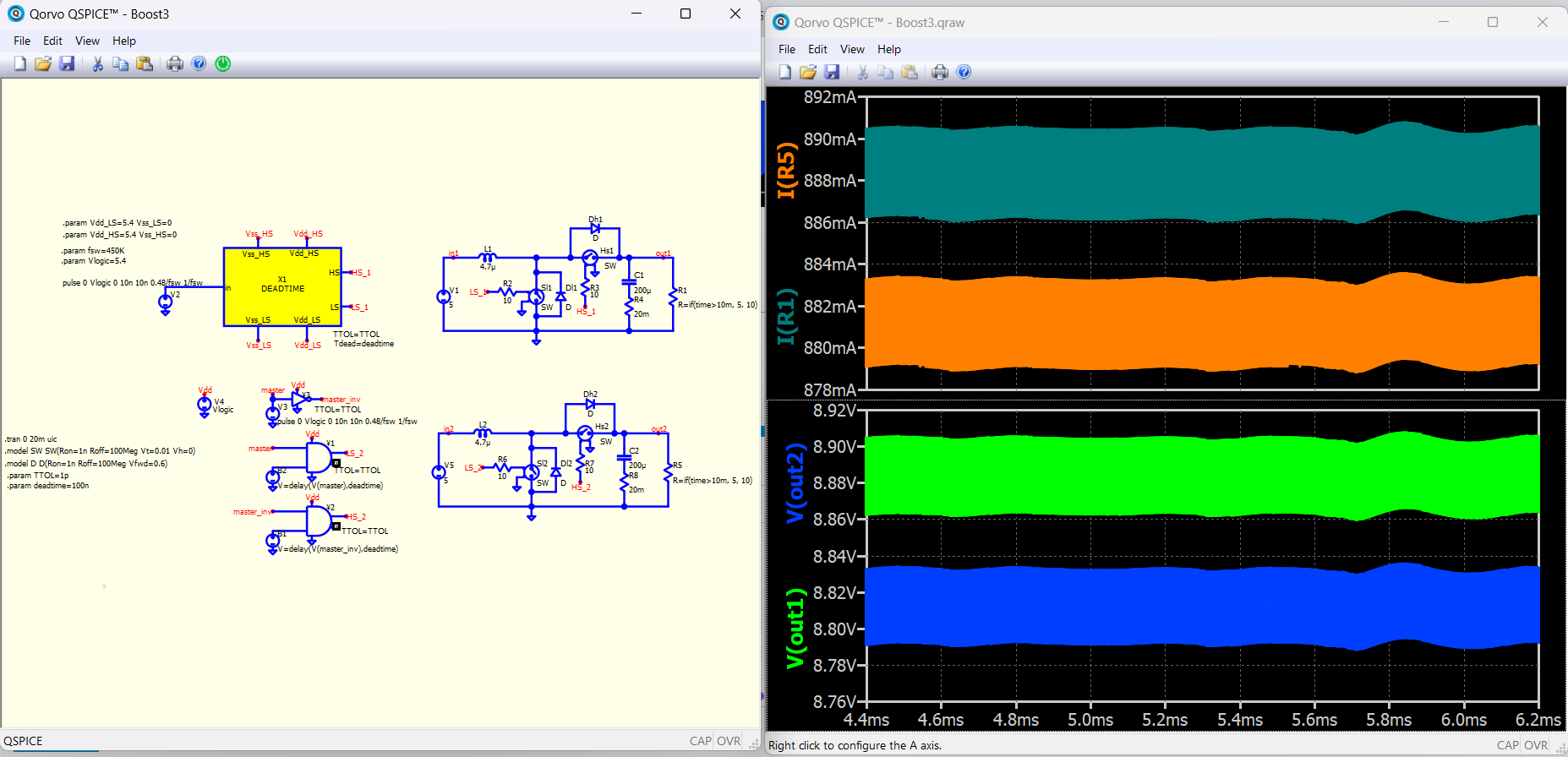
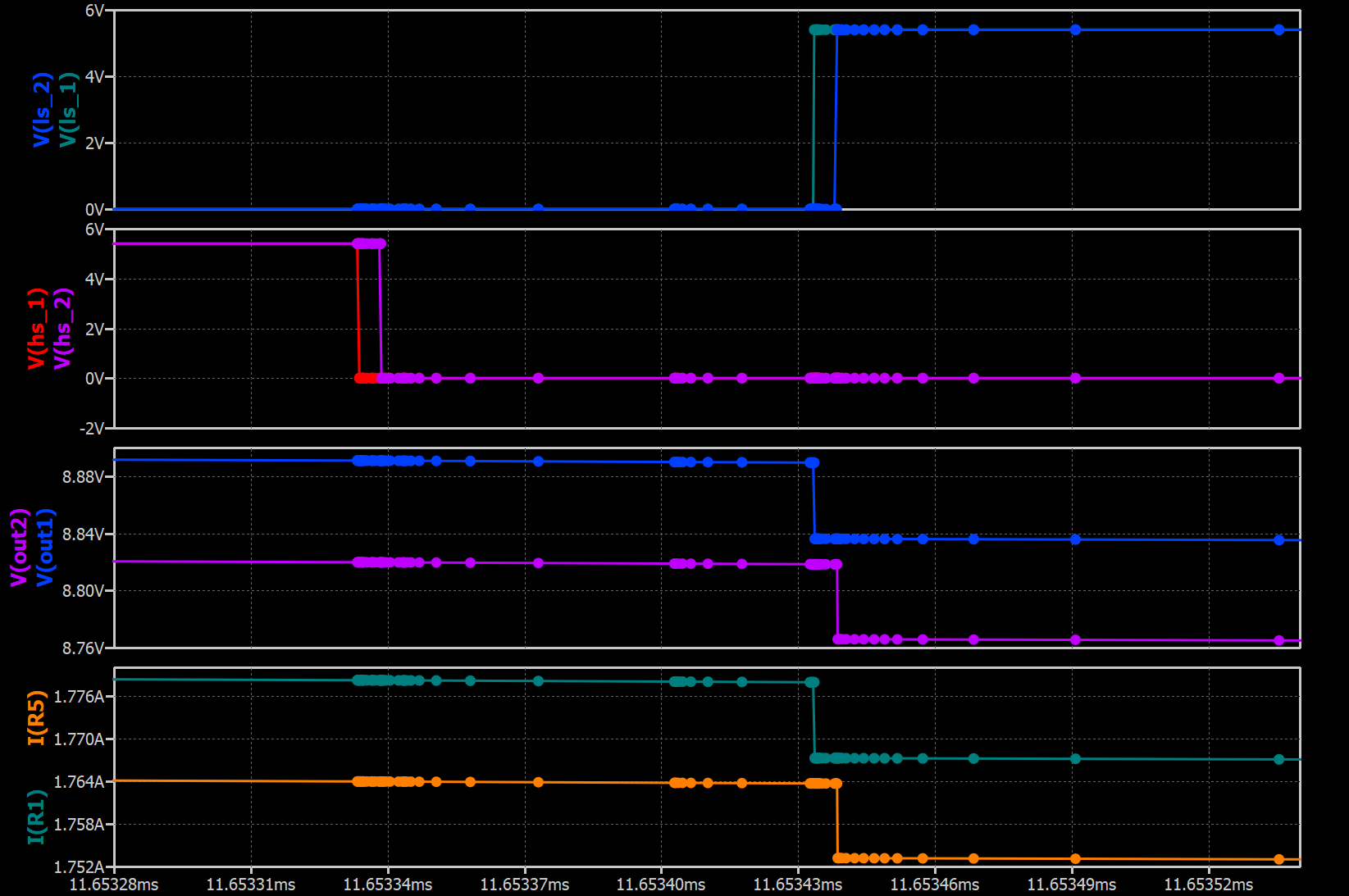
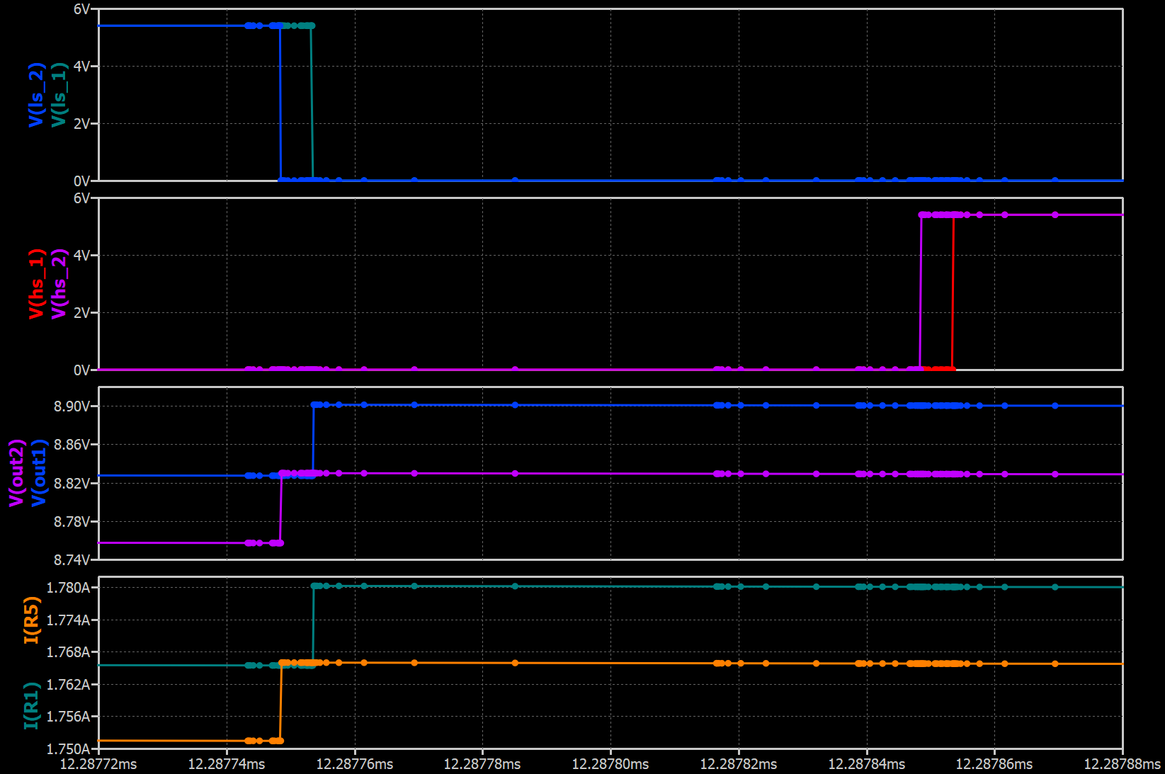
@KSKelvin From the above reason comes the difference and why the graphs not match exactly. Question: how to make LS_1 to match LS_2 (or the other way around, how to make both LS_2 to match LS_1). The same question for HS_1 and HS_2.